
Some inventions don’t just improve a technology; they redefine the entire industry’s direction. US9130074B2 stands out for doing exactly that.
It introduces a solar cell architecture that leverages multifunctional layers and single-side deposition techniques to improve both performance and manufacturing efficiency. This patent has recently been cited in a case involving First Solar, Inc. v. JinkoSolar Holding Co., Ltd., serving as a reminder of its broader relevance in the solar industry.
In this article, we utilize the Global Patent Search (GPS) platform to identify technologies that align with the key concepts underlying US9130074B2. Instead of focusing on the legal backdrop, we zero in on related patents that reflect similar technical structures. If you’re involved in solar innovation or IP strategy, this data-first approach offers valuable insight into where the field is headed.
Understanding Patent US9130074B2
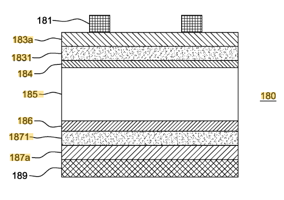
US9130074B2 focuses on solar cell architectures designed to maximize efficiency while streamlining manufacturing. The invention integrates multiple functional layers, such as conductive, antireflective, and passivation films, onto a central substrate. These layers are engineered to perform several roles simultaneously, including carrier flow, light transmission, and surface protection. The patent also outlines advanced fabrication methods like one-sided CVD deposition and high-temperature treatments to form or convert these layers effectively.
Source: Google Patents
Its four key features are
#1. Multifunctional layers: Serve as passivation, junction, conductive, and antireflective components in a single structure.
#2. Single-side CVD processing: Enables precise layer application on one surface, reducing complexity and cost.
#3. Thermal treatment activation: Crystallizes layers and activates dopants through controlled high-temperature exposure.
#4. Integrated layer efficiency: Uses combined structures to reduce recombination losses and enhance vertical carrier transport.
This patent reflects critical advancements in solar cell design, balancing high performance with cost-effective production. Its methods and structural concepts are particularly relevant to evolving standards in photovoltaic engineering, especially in applications where layered materials and simplified processing are key.
For a broader view of how next-generation energy technologies are shaping global sustainability, explore our feature on leading green-tech innovators driving breakthroughs in energy and mobility.
Similar Patents As US9130074B2
To explore the innovation landscape surrounding US9130074B2, we ran the patent through the Global Patent Search tool. Below is a quick glimpse of the GPS tool in action:

Source: Global Patent Search
This analysis surfaced a list of related patents that share technical similarities in layered solar cell structures, deposition techniques, and junction integrity. Below, we highlight five of these references that reflect comparable ideas in photovoltaic engineering. These examples offer insight into how similar challenges have been addressed across different systems.
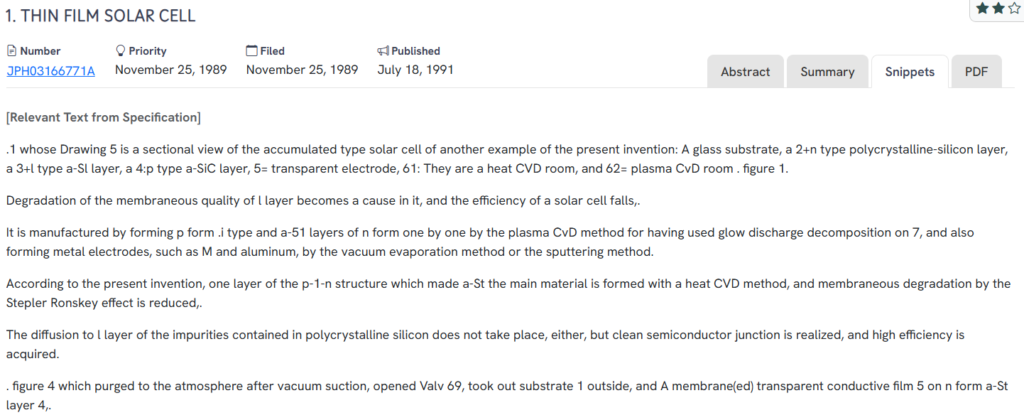
#1. JPH03166771A
This Japanese patent JPH03166771A, published in 1991, describes a multi-layer thin-film solar cell composed of polycrystalline and amorphous silicon layers. It incorporates both heat CVD and plasma CVD methods for deposition, with an emphasis on preventing membrane degradation and preserving the quality of the semiconductor junction.
Source: GPS
What this patent introduces to the landscape?
- Layered p-i-n structure – Combines polycrystalline silicon, amorphous silicon (a-Si), and amorphous silicon carbide (a-SiC) to build a structured solar junction.
- Heat and plasma CVD deposition – Utilizes both thermal and plasma-assisted deposition for forming silicon layers.
- Membrane quality optimization – Reduces degradation effects like the Stepler Ronskey phenomenon and prevents impurity diffusion from polycrystalline layers.
- Transparent conductive film – Applies a transparent electrode over the active layers to enable light penetration and electrical conduction.
A similar material-engineering approach appears in our analysis of US8337725B2,
play a central role in improving device performance.
How it connects to US9130074B2?
Both patents prioritize efficiency through multilayer construction and controlled deposition techniques. JPH03166771A complements US9130074B2 by showcasing early use of heat CVD and plasma CVD to fabricate layered junctions with minimal degradation, an approach echoed in US9130074B2’s multifunctional films and thermal treatment processes.
Why this matters?
This prior art reinforces the significance of deposition control and junction integrity in solar cell innovation. Its combination of thermal and plasma processes anticipates the multifunctional layer approach seen in US9130074B2, highlighting a shared emphasis on efficiency through precise material layering.
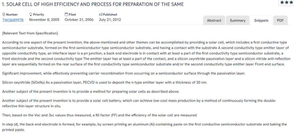
#2. TWI368997B
This Taiwanese patent TWI368997B, published in 2012, describes a high-efficiency solar cell structure incorporating a pn junction, passivation layers, and advanced front/rear electrode configurations. It outlines a process optimized for reducing carrier recombination and enabling scalable manufacturing.
Source: GPS
What this patent introduces to the landscape?
- Integrated pn junction design – Forms an emitter layer of opposite conductivity directly on a semiconductor substrate to create an efficient junction.
- Silicon oxynitride passivation layer – Uses SiOxNy as a passivation barrier to suppress carrier recombination at the surface.
- Anti-reflective silicon nitride coating – Enhances light absorption by reducing surface reflection.
- PECVD-based emitter deposition – Applies the emitter layer using plasma-enhanced chemical vapor deposition for better layer control.
- Low-cost electrode formation – Implements screen printing of aluminum-based paste for scalable back-end electrode processing.
How it connects to US9130074B2?
Both patents emphasize high-efficiency solar cell architecture through advanced layer integration and surface engineering. TWI368997B aligns with US9130074B2 in its use of PECVD for precise film deposition, surface passivation strategies, and practical methods for mass production.
Why this matters?
This reference demonstrates how integrating passivation and anti-reflection coatings with scalable manufacturing can boost solar cell efficiency. It mirrors the foundational themes in US9130074B2, namely, layer efficiency, doping control, and production scalability, making it a relevant prior art in the landscape of solar innovation.
Note: US9130074B2 mirrors US10391344B2 Patent Audit’s validation logic. Both ensure systems withstand operational strain while preserving safety and consistent performance.
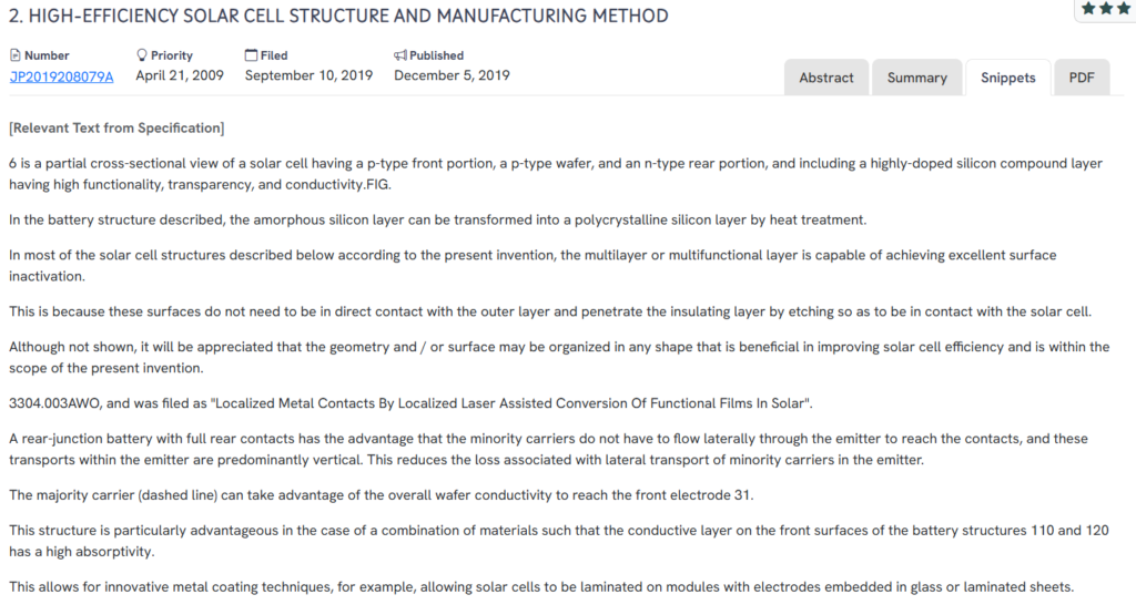
#3. JP2019208079A
This Japanese patent JP2019208079A, published in 2019, presents a solar cell architecture utilizing multifunctional layers, thermal processing, and vertical carrier transport mechanisms to achieve improved energy conversion. It emphasizes rear-junction configurations and embedded electrode techniques for optimizing both efficiency and manufacturability.
Source: GPS
What this patent introduces to the landscape?
- Rear-junction structure with vertical carrier flow – Minimizes lateral resistance by guiding minority carriers directly to rear contacts.
- Multifunctional silicon compound layers – Combines passivation, conductivity, and optical functionality in a single layer.
- Thermal treatment for dopant activation – Uses heat to crystallize amorphous silicon and diffuse dopants to form high-low or pn junctions.
- Innovative electrode embedding – Describes electrodes embedded in glass or laminate sheets for improved mechanical integration.
- Localized layer positioning under contacts – Optimizes optical performance by isolating conductive layers to contact zones, reducing absorption losses.
How it connects to US9130074B2?
JP2019208079A closely mirrors US9130074B2 in its use of heat-activated multifunctional layers, vertical current flow designs, and multifunctional coatings. Both patents aim to enhance efficiency through thoughtful layering and manufacturing strategies that address both optical and electrical performance.
Why this matters?
This reference underlines the benefits of rear-junction solar cells and multifunctional coatings, two pillars of the architecture claimed in US9130074B2. Its combination of structural and processing techniques reinforces the broader trend of optimizing solar cell performance through integrated design and fabrication control.
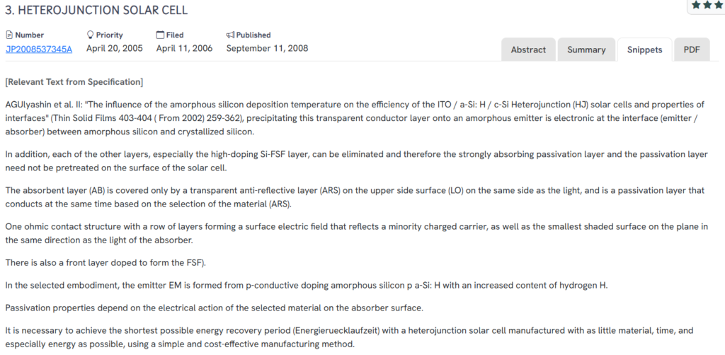
#4. JP2008537345A
This Japanese patent JP2008537345A, published in 2008, outlines a heterojunction solar cell structure that combines amorphous and crystalline silicon layers to improve interface efficiency. It emphasizes low-temperature plasma CVD processes and material selection to minimize energy use and manufacturing complexity.
Source: GPS
What this patent introduces to the landscape?
- Heterojunction design using amorphous/crystalline silicon – Forms a junction between p-type amorphous silicon and crystalline silicon to enhance carrier separation.
- Low-temperature plasma CVD processing – Deposits emitter and anti-reflective layers at temperatures between 250 °C and 350°C, reducing energy consumption during fabrication.
- Integrated passivation and anti-reflection – Utilizes material choices that offer both passivation and light management from a single layer (ARS).
- Minimized surface shading and contact optimization – Implements a contact structure that reflects minority carriers and reduces shadowing losses.
- Material-efficient manufacturing approach – Focuses on achieving a short energy payback time by simplifying fabrication and minimizing resource input.
How it connects to US9130074B2?
Both patents focus on interface engineering between layers, efficient deposition strategies, and multifunctional surface coatings. JP2008537345A complements US9130074B2 by demonstrating how junctions can be enhanced with minimal materials and energy, aligning with the US9130074B2’s emphasis on simplified, high-efficiency manufacturing techniques.
Why this matters?
This patent highlights the importance of optimizing silicon interfaces and integrating passivation with anti-reflective properties in a compact structure. It echoes US9130074B2’s goals of boosting solar performance while reducing fabrication complexity, key concerns in scalable photovoltaic design.
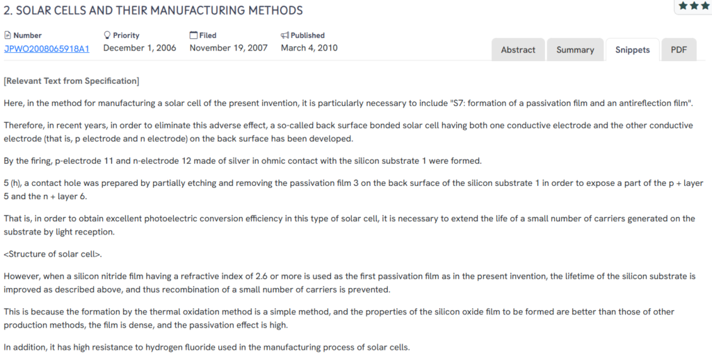
#5. JPWO2008065918A1
This Japanese patent JPWO2008065918A1, published in 2010, presents a method for manufacturing solar cells with an emphasis on rear-side electrode placement and advanced passivation techniques. It details how passivation and anti-reflective films are integrated to enhance carrier lifetime and overall conversion efficiency.
Source: GPS
What this patent introduces to the landscape?
- Rear-contact solar cell structure – Positions both p-type and n-type electrodes on the rear surface to reduce front-side shading and enhance light absorption.
- Dual-layer passivation and anti-reflection films – Uses silicon nitride with a refractive index above 2.6 to provide high passivation and reduce carrier recombination.
- Contact hole etching – Describes a precise method for forming contact holes through passivation layers to expose doped regions without compromising substrate integrity.
- Thermal oxidation-based silicon oxide film – Applies a dense, high-quality oxide layer via thermal methods for superior passivation performance.
- Chemical resistance and durability – Highlights the material’s robustness against HF (hydrogen fluoride), a common processing chemical in solar cell manufacturing.
How it connects to US9130074B2?
This reference shares technical parallels with US9130074B2 in its focus on effective passivation strategies, rear-junction design, and multilayer film integration. Both emphasize extending carrier lifetime and simplifying manufacturing steps using proven thermal and deposition techniques.
Why this matters?
JPWO2008065918A1 contributes valuable insight into the role of material choice and structural design in improving solar cell performance. Its combination of rear-contact layout and advanced passivation supports similar goals outlined in US9130074B2: efficient, manufacturable, and high-performing solar technologies.
How to Find Related Patents Using Global Patent Search?

Understanding the broader innovation landscape surrounding a solar cell patent can be crucial for enhancing photovoltaic efficiency, refining manufacturing methods, or evaluating layered cell structures. The Global Patent Search tool streamlines this exploration, making it easy to spot inventions with similar architectures, material strategies, or processing techniques. Here’s how it works:
1. Enter the patent number into GPS: Start by entering a patent number like US9130074B2 into the GPS tool. The system transforms this into a smart query, which can also be refined using material-specific terms such as “CVD deposition” or “passivation layer.”

2. Explore conceptual snippets: GPS now highlights intelligent snippets rather than mapping features line by line. These excerpts capture technical patterns, like thermal treatment processes or multi-functional silicon layers, showing how they appear in other patents.
3. Identify related inventions: The tool surfaces patents that reflect similar photovoltaic design logic, be it rear-junction configurations, dopant activation methods, or surface passivation techniques, offering a broader view of how solar innovations are evolving.
4. Compare methods, not legal claims: GPS emphasizes system behavior and technical execution. It focuses on engineering parallels rather than interpreting legal language or the scope of claims.
5. Accelerate discovery in photovoltaics: Whether you’re researching thin-film cells, heterojunctions, or industrial manufacturing routes, GPS helps uncover patents that might otherwise remain hidden across disparate sectors.
With this approach, Global Patent Search provides researchers, engineers, and IP professionals with a practical, concept-driven view of related solar technologies, supporting sharper IP strategies and deeper technical insights.
Disclaimer: The information provided in this article is for informational purposes only and should not be considered legal advice. The related patent references mentioned are preliminary results from the Global Patent Search tool and do not guarantee legal significance. For a comprehensive related patent analysis, we recommend conducting a detailed search using GPS or consulting a patent attorney.