Ever dropped your phone and wondered how the chip inside still works perfectly?
That little miracle depends on how well its internal chip package is built. The chip package, for those uninitiated, is a sealed structure made of metal and molding material that protects the circuit from stress, heat, and shock.
But over time, even the toughest packages can crack from within. Microscopic gaps form between the metal frame and the molding compound, causing connections to weaken and signals to fail.
That is the challenge US8258611B2 set out to solve.
The patent introduced a new leadframe structure that prevents delamination and keeps electrical bonds strong even under pressure.
To understand how this innovation fits into the evolution of reliable chip design, we used the Global Patent Search tool. It revealed a network of related ideas shaping how modern electronics stay durable and dependable.
Understanding the Science Behind US8258611B2
Every chip sits on a small piece of metal called a leadframe. It holds the chip in place, connects it to other components, and helps protect it from stress and heat.
But the same structure that keeps everything together can also become its weakest link. When the leadframe and the molding compound separate, even slightly, it leads to delamination, a tiny gap that can break wire connections and cause the chip to fail over time.
US8258611B2 focuses on solving exactly that problem. It introduces a smarter leadframe design where a special barrier area sits between the die-pad (which supports the chip) and the bonding area (where wires connect). This barrier is not just structural, it is also electrical. It connects both sides while blocking the spread of delamination.
The result is simple but powerful. A chip package that stays bonded longer, performs more reliably, and resists the mechanical stress that usually leads to cracks.
Here are the key Features of US8258611B2
- Barrier-based connection: The patent adds a narrow barrier area that links the die-pad and bonding area, reducing stress buildup and preventing delamination from growing.
- Optimized shape and width: The barrier is long and narrow, designed to redirect mechanical stress instead of letting it expand across the surface.
- Improved wire bonding: The bonding area remains stable during thermocompression, which keeps bond wires intact even under high temperature cycles.
- Enhanced reliability: By containing delamination before it spreads, the structure ensures long-term electrical performance.
- Flexible integration: The concept can be adapted to different chip packages, including Dual In-Line, Quad Flat, and Small Outline designs.
Together, these features turn a common failure point into a source of strength, creating a subtle design improvement that keeps modern electronics dependable for years.
Exploring the Web of Connected Innovations In Chip Packet Design
Every breakthrough stands on the shoulders of earlier ideas. To understand how this leadframe structure evolved, we looked at patents that tackled similar challenges in chip packaging and electronic reliability.
Let’s have a look at some of them:
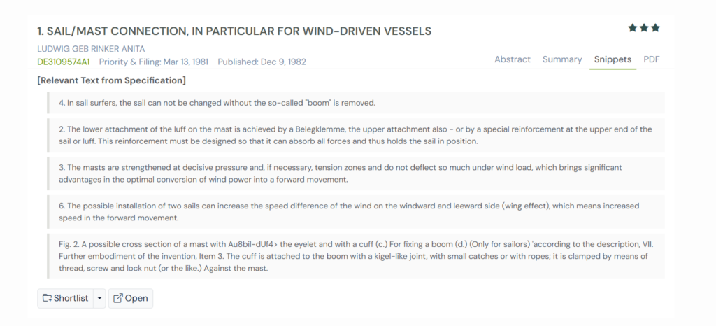
1. DE3109574A1 – Sail and Mast Connection System
Published in 1982, the patent might seem far from semiconductor design at first glance. But it shares the same principle that drives US8258611B2: stability under stress.
The invention describes a way to connect sails to masts more securely on wind-driven vessels. Traditional sail systems risked loosening or tearing under pressure. This patent solved that by reinforcing the mast at key stress points and redesigning how the sail attached, allowing it to hold firm even in strong winds.
The logic is simple. When you control how forces move through a structure, you prevent damage before it begins.
That same thinking echoes in US8258611B2. Instead of wind pressure, it deals with thermal stress inside chips. By strengthening weak points and managing stress flow, both inventions aim for the same goal i.e. lasting performance through smarter design.
The Bigger Picture
Engineering challenges often look different on the surface but follow the same physics underneath. Whether it is a sail catching the wind or a chip enduring heat cycles, both depend on how well the structure handles stress.
This early idea of reinforcing pressure zones laid the foundation for reliability-driven designs like US8258611B2, proving that durability starts with balance.
2. JPH02106837U – Leadframe for Improved Resin Adhesion in IC Packages
Published in 1990, the patent focuses on enhancing how resin adheres to metal leads in semiconductor packaging. In traditional IC packages, especially Dual In-Line Packages (DIP), weak adhesion between the resin and lead portions often caused peeling or delamination when the package was bent or exposed to stress.
To solve this, JPH02106837U introduced structural changes to the inner lead portion, improving the bond between resin and metal. By strengthening this interface, it prevented separation during molding or later mechanical stress, ensuring the chip package remained intact through handling and operation.
This invention connects closely with US8258611B2, which took this idea further by addressing delamination on a more microscopic, barrier-based level.
While the Japanese patent focused on adhesion strength through surface design, US8258611B2 refined the structural layout itself, isolating stress zones to prevent delamination growth altogether.
The Bigger Picture
JPH02106837U represents one of the earliest efforts to combat delamination in IC packages, a problem that has persisted across generations of semiconductor designs.
Its focus on adhesion chemistry laid the groundwork for later innovations like US8258611B2, where the emphasis shifted toward stress management and long-term reliability. Both demonstrate how even minor interface tweaks can lead to major leaps in electronic durability.
3. JP2563507Y2 – Semiconductor Device with Enhanced Wire Bonding Stability
Published in 1998, the patent looks at something that might sound tiny but matters a lot in chip packaging. It focuses on how the chip connects to the leadframe through thin bonding wires.
In older designs, many of these leads were slightly raised above the chip surface. That meant engineers had to create tall wire loops to make the connections work. The result was thicker packages, more material use, and higher chances of damage or wire shifting during molding.
JP2563507Y2 fixed that problem with a smarter design. It added a special mounting cage for the chip and used thin insulating layers between different groups of leads. This made the leads more stable, reduced the height of those delicate wire loops, and made the whole process more reliable and cost efficient.
If you look at it next to US8258611B2, you can see they share the same goal of making chip packages last longer. The Japanese patent improved the physical layout and insulation so bonding stayed strong, while US8258611B2 added a barrier inside the structure to stop delamination before it spreads. Both are about one thing, keeping chips reliable even after years of use.
The Bigger Picture
The patent shows how even small design choices can make a big difference in semiconductor reliability. By rethinking how bonding wires are arranged and supported, JP2563507Y2 made chips easier to build and less likely to fail.
Together with US8258611B2, it tells the story of how chip engineers learned to manage stress, alignment, and stability through smarter structures and thoughtful engineering.
Recommended Read: Explore how US10637142B1 applies similar reliability principles at the network level, using steerable antennas and edge computing to make 5G communication faster and more resilient.
4. US6091135A – Lead Frame with Pre-Mold Paddle for Better Chip Reliability
Filed in 1997 by LG Semicon, this patent solved a recurring issue of delamination in chip packaging. In traditional designs, the chip sat on a copper paddle sealed inside epoxy. Since the two materials expand differently under heat, small gaps would form over time, causing cracks and lower reliability.
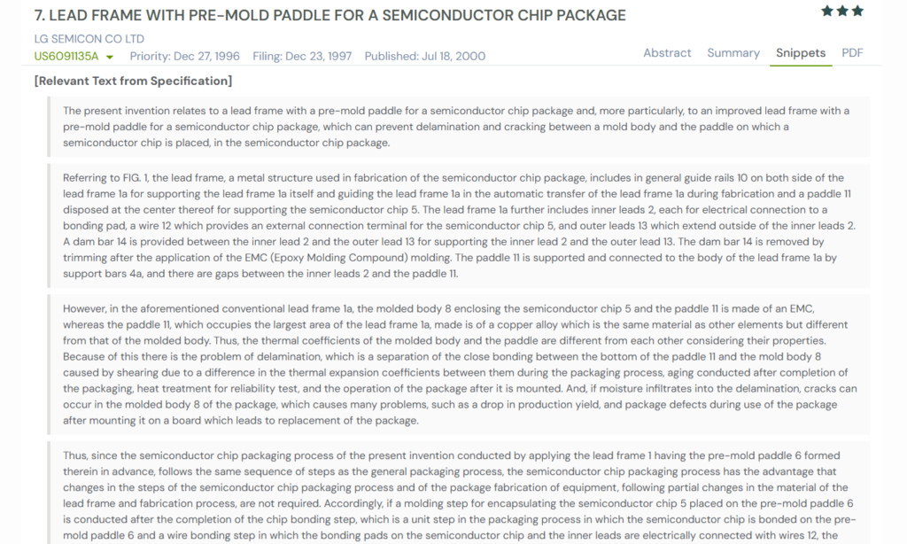
US6091135A fixed this by introducing a pre-mold paddle made from the same material as the epoxy mold compound. Because both had identical thermal properties, the risk of separation disappeared. The new setup required no major process changes and immediately improved chip yield and long-term stability.
The Bigger Picture
Reliability often comes from small material tweaks. This design showed that matching properties, not just changing structure, can make chips stronger and last longer.
5. JPH11233708A – Lead Frame and Semiconductor Device Designed to Prevent Wire Breakage
Filed in 1999 by Hitachi, the patent tackled a subtle but serious problem in wire bonding. In traditional chip packages, tiny bonding wires connect the chip to the leadframe. During molding or heat cycles, these wires can crack or break, especially near the second bond point where stress is concentrated.
The patent introduced a simple but clever change. It added fine grooves to the inner leads where the wires attach. These grooves helped absorb thermal stress and strengthened the crimping area, making it harder for wires to snap under pressure.
Just like US8258611B2, this design focused on reliability through structural precision. While US8258611B2 handled delamination between materials, JPH11233708A made the bonding joints themselves more durable.
The Bigger Picture
Both ideas show how chip reliability often depends on microscopic details. A single groove or barrier, placed in the right spot, can make the difference between a device that fails early and one that lasts for years.
Comparison Summary: How Each Patent Relates to US8258611B2
When viewed together, these patents reveal how innovation in one field can inspire solutions in another. Each builds on the same foundation as US8258611B2, designing for reliability, stability, and long-term performance.
| Patent | Core Focus | Technical Overlap with US8258611B2 | The Broader Picture |
| DE3109574A1 (Ludwig Geb Rinker Anita) | Reinforced sail–mast connection system that stays stable under heavy wind pressure. | Both focus on managing stress within a structure to prevent cracks or separation under load. | Showed how controlling force distribution strengthens performance, a concept later mirrored in micro-scale chip packaging. |
| JPH02106837U (Japan) | Improved resin adhesion between metal leads and molding compounds in IC packages. | Both aim to reduce delamination. This one does it through better surface adhesion, while US8258611B2 introduces a barrier to contain stress. | Early foundation for delamination control in semiconductors, proving that stronger adhesion leads to longer-lasting packages. |
| JP2563507Y2 (Japan) | Redesigned leadframe layout to stabilize wire bonding and reduce loop height in semiconductor chips. | Both improve reliability by reinforcing internal structure. This patent optimized wire layout; US8258611B2 added a stress-blocking barrier. | Highlighted the shift toward precise structural design, making chips thinner, stronger, and more reliable. |
| US6091135A (LG Semicon Co. Ltd.) | Introduced a pre-mold paddle made from the same material as epoxy to stop delamination. | Both target separation failures. This one prevents thermal mismatch through material selection; US8258611B2 prevents crack spread through geometry. | Demonstrated how material harmony can solve mechanical stress problems, a key principle in packaging innovation. |
| JPH11233708A (Hitachi Ltd.) | Added grooves in inner leads to prevent wire breakage under thermal stress. | Both reinforce fragile points to withstand stress. One strengthens bonding joints; the other protects the chip-mold interface. | Emphasized microscopic precision as the backbone of semiconductor durability, small details that ensure long-term stability. |
Taken together, these patents show how one idea, i.e., managing stress to improve reliability, has evolved across decades of semiconductor engineering.
The story doesn’t end there.
US8258611B2 continues to stay relevant, even beyond the lab, as it’s currently active in litigation in the Texas Eastern District Court. Its involvement in real-world legal disputes underlines just how valuable and widely adopted its core design principles have become across the chip industry.
Discovering Connections with the GPS Tool
Every patent exists as part of a larger story of innovation. The Global Patent Search tool helps uncover that story.
It builds a broader landscape of related inventions, showing how one idea evolves across time, materials, and industries.

Here’s how the tool works:
- Begin with your core invention: Enter a patent number, such as US8258611B2, or describe it in simple words. For example, a leadframe design that prevents delamination in electronic packaging. GPS uses that as a starting point to find related patents exploring similar challenges, like structural stress control or adhesion improvement.
- Review the highlights: The tool presents short summaries from claims and descriptions that match your topic. GPS also shows snippets that show where each reference overlaps, maybe a new bonding method, a novel material mix, or an alternative way to manage heat and stress.
- Dive deeper where needed: When a result looks relevant, you can open the full document to study how the structure, material, or connection method differs. This helps you trace how the idea of stress reduction in chips evolved over years of experimentation.
- Look beyond one field: GPS reveals patterns that extend beyond semiconductors, from wind power systems to air conditioning units. It shows how the same engineering principle of managing stress and maintaining stability is reimagined across industries.
Unlike other traditional patent search tools, GPS goes beyond keywords. It maps how ideas influence each other. For US8258611B2, it highlighted how a simple concept connects innovations in materials science, electrical engineering, and renewable energy.
Try the GPS tool today to explore these connections for yourself!